MEMS technology
In the previous section (part 2) we got to know the vibration measuring method. This section deals with the establishment of MEMS technology at TrueDyne Sensors AG. The technology has brought about the MEMS sensor, the heart of which is an oscillating silicon measuring channel. Compared to conventional resonator technology, it combines numerous advantages. These range from its small size and a wide range of applications to the exact determination of the density of gases, even at low pressure, and an extremely fast reaction time.
Contents
- What is MEMS technology?
- Where are MEMS technologies used?
- How is the Omega chip structured?
- What opportunities does MEMS technology offer?
What is MEMS technology?
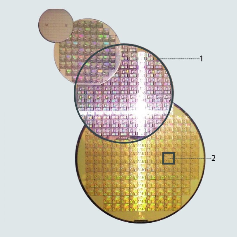
For the semiconductor technology, several electronic components are structured on a semiconductor substrate (often made of silicon) using various process technologies, e.g. photolithography and thin-film technology, and assembled into a chip. Since the individual steps for the production of a chip are very complex, these steps are multiplied and several chips are produced simultaneously. This is done with a circular or square, disc-shaped wafer which consists of the material of the required substrate.
Semiconductor technology allows for the miniaturization of electronic circuits, which in classic electronics consist of mechanically manufactured components. One TrueDyne Sensors AG MEMS chip not only includes electronic but also mechanical and fluidic functions.
Due to the high demands on the individual components, a TrueDyne Sensors AG MEMS chip is usually not limited to a silicon substrate. Instead, diverse materials are used for the different components, which are brought together using various assembly and connection techniques.¹

Circular wafer – Source: https://de.wikipedia.org/wiki/Wafer
Where are MEMS technologies used?
How has MEMS technology developed at
TrueDyne Sensors AG?
This system has not proven itself effective for measuring the flow rate at TrueDyne Sensors AG. However, it has been shown that the vibrating silicon channel can be used very effecticely as a resonator densimeter .
How is the TrueDyne Sensors AG MEMS chip constructed?
The TrueDyne Sensors AG MEMS chip is manufactured using a total of four wafers:
- Two silicon wafers form the measuring channel. The measuring channel is formed using plasma etching technology. For this purpose, half of each channel is etched into a silicon wafer. The channel is created by connecting the two halves (bonding method).
- A glass wafer contains metallic electrodes, fluidic openings and the temperature sensor.
- Another silicon wafer is used to package the measuring channel in a vacuum. This allows the measuring channel to oscillate without air damping.
How is the TrueDyne Sensors AG MEMS chip constructed?
Miniaturization is gaining ground particularly in applications where small sample quantities and a compact structure are of great importance.
The thermal and mechanical properties of silicon mean that a powerful sensor is also provided.
Silicon is a good conductor of heat. The channel is therefore not exposed to large temperature differences. The temperature information required for density measurement can thus be determined precisely and easily.

TrueDyne Sensors AG MEMS-Chip – Source: TrueDyne Sensors AG
The silicon channel can vibrate at a very high frequency. This leads to a short measuring time and makes the measuring signal independent of external, mechanical interference vibrations.


